These days, single and double layer boards bring no material differences in cost or manufacturing processes.
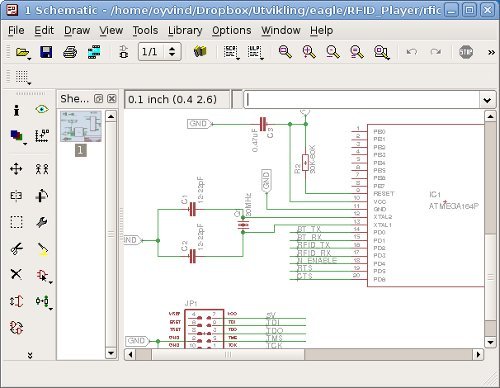
Download Schematic To Pcb Layout Pictures. How to place your components. You've done your usual excellent job of putting together the pcb schematic.
PCB Design - How To Create Circuit Boards - Build ... from www.build-electronic-circuits.com
Hello diy'ers, i will share the schematic and pcb layout for fullbridge with pfc (power factor correction) switching mode power supply. This repository contains schematics and board layouts for all of smac modules and development platforms. Pcbgogo has a professional pcb layout team with over 10 years experience, and make a brief introduction what is pcb layout, learn pcb layout process and capability , and what pcbgogo they have the ability to finish the whole design process from drawing the schematic to assembly.
The user can select whether the parts are to go into a component bin, or.
Da14580 checklist for schematic and pcb layout. Most eda vendors can provide bundled schematic capture and pcb layout packages that are designed to work together. The efficient laying out of traces on a pcb is a complex skill, and requires much patience. There is an easy order process that quotes your board as you design.