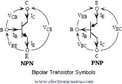
Download Bipolar Transistor Schematic Symbol Background. The construction and circuit symbols for both the npn and pnp bipolar transistor are given above with the arrow in the circuit symbol always showing the direction of conventional current flow. Phototransistors come in npn and pnp varieties.
Ebers Moll Model of a Bipolar Transistor - Electronics Area from electronicsarea.com
Look at the diagram below. In the year 1904 j.a. Phototransistors come in npn and pnp varieties.
This means that interchanging the collector and the the diagram opposite is a schematic representation of a pnp transistor connected to two voltage sources.
Allows current flow when high potential at base (middle). The transistor is the main building block element of electronics. A bipolar junction transistor (bjt) has three terminals connected to three doped semiconductor regions. The base, the collector, and the emitter.