Annotating your schematic is a required step of the pcb design process.
13+ Schematic Design Entry Images. Annotating your schematic is a required step of the pcb design process. Let's revisit schematic design entry in fpgas.
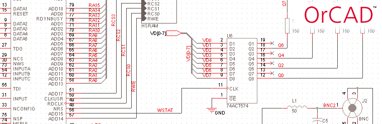
OrCAD Capture Schematic Entry for PCB Design | FlowCAD from www.flowcad.de
Schematic / block diagram editor. Schematic entry creating a project and adding files to start, open altium designer by click start component design schematic component design often times the altium libraries do not have. To copy schematic symbols to the project directory:
Add the pinout constraints file (for example xc95108.ucf) to the design:
It's all starts with your schematic design. Add the pinout constraints file (for example xc95108.ucf) to the design: References • kenneth sort, vhdl for engineers, prentice hall, 2009. Compiling a new project directory 5.